A delayed AVC with DC amplification for the 51J-5
~ It may also be applicable to other receivers ~
| Preamble:
After this receiver was bought, I noticed that the AVC didn't really exist as such, what there was was something similar to the injection of two voltage levels into the AVC, a medium one for medium signals in 'Fast', a high one for strong signals in 'Slow' (in this position the sensitivity of the receiver was significantly reduced), and for normal listening the radio had to work with AVC 'Off'.
When drawing the existing AVC circuit it became clear that it had been badly modified with who knows what intention. It is also not clear that mod comes from the army (51J-5s are certainly from military use), IMO it was modified by some previous owner who had the usual objections on SSB reception and didn't like messing with RF gain. There is a lot of creativity in adapting AGC circuits designed for AM to SSB reception, but there is no easy trick based on changing a couple of components and making a couple of connections (if it were that easy, the manufacturer's engineers would have already included it).
Several AGC designs were initially tested in order to restore standard AVC operation, but it was concluded that the one best suited to the 51J-5 was the one based on the existing remains of the original design (similar to 51J-4). The restoration of the AVC circuit in the 51J-5 has been based on the clue provided by these remains, the comparison with that of the 51J-4, and the search for possible compatible designs.
|
Step 1.- Looking for something similar to the remains of the existing 51J-5 circuit, and the 51J-4 AVC circuit:
|
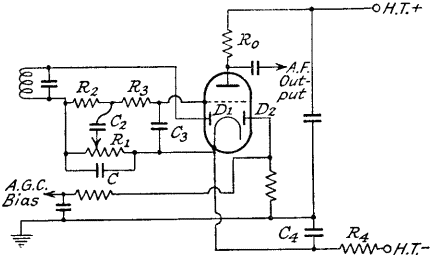 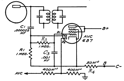 |
| DC Amplified delayed AGC designs found. On the left, a design from a Sturley's book(1), combining AGC output with AF output and volume control. On the right, an AGC output-only design from a Rider book(2). This is the closest to what was found in 51J-5. Diagrams have been slightly revised for better explanation and understanding. |
| The main difference between the AGC (AVC) voltage source of 51J-4 and 51J-5:
The AVC system of 51J-4 combines AVC with RF gain, 51J-5 has the AVC system separated from the RF gain circuit, same as 75A-4. Another peculiarity is that the AGC output in the 51J-4 is through the plate of the DC amplifier, and in the 51-5 through the cathode adding an output diode to prevent any possible positive voltage, just like the AGC systems shown above. |
| AC/DC 'signal' differences.
Pure DC amplification means that the only thing that will be processed are voltage levels (more positive or less negative, more negative or less positive), therefore a DC circuit will work more electrically than electronically, the 'signal' concept is different here. Therefore, by making point
measurements on a resistor placed between a positive and a negative pole, the only thing that will happen is that the voltage at that point will be more or less positive, or more or less negative, regarding "something" (ground in the circuit below). This is the key to understanding the DC amplified AGC system. Do not confuse this with DC coupling in AF amplifiers.
|
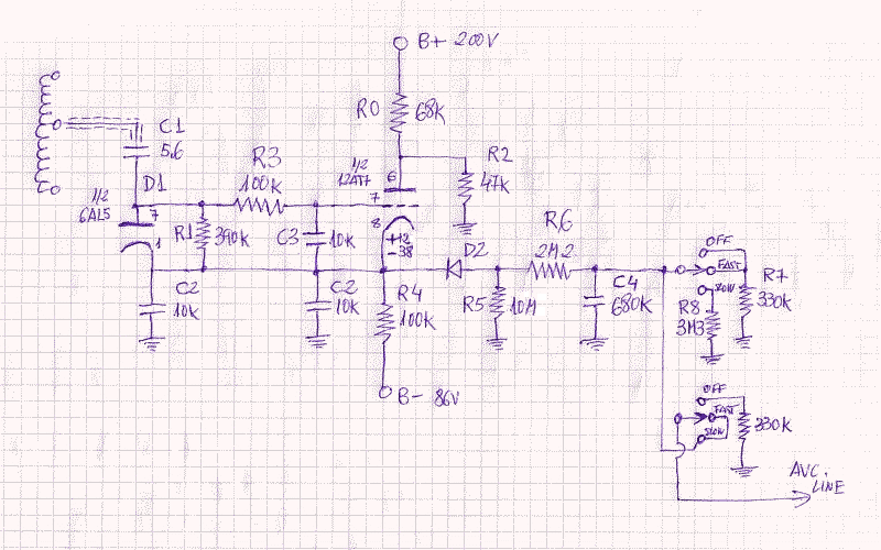
| Step 2.- Adapting the circuit. What was there before, and what is there now: |
A DC amplified AGC (AVC) design for AM and SSB
Hover over the schematic below to see the circuit as found.
| RF input (signal) |
AGC rectifier (D1) |
Effect at grid |
Current inside tube (its resistance varies) |
Voltage at the output diode (D2) |
| Low level RF signal |
Negative rectified voltage is low |
Grid has low negative voltage, triode resistance (Ri) is low. |
Current is high, cathode very positive. |
It does not conduct, inside delay time. D2 blocks the + voltage. |
| Medium level signal - downward trend. |
Negative rectified voltage is still low |
Grid has more negative voltage, but insufficient to break delay voltage. |
Current is medium, cathode still positive. |
It still does not conduct |
| Medium level signal - upward trend. |
Negative rectified voltage is enough |
Grid has enough negative voltage to overcome delay voltage |
Current is low, cathode zero or negative. |
It conducts some negative voltage |
| High level RF signal |
Negative rectified voltage is high |
Grid has a lot of negative voltage, triode resistance (Ri) is high. |
Current is very low, cathode very negative. |
It conducts a lot of negative voltage |
| |
| R0: Plate load |
R2: Voltage divider |
D1: AGC rectifier |
R1: D1 load |
C1: IF inlet, 5.6 pF only! |
D2: AGC output polarity controller (never +)
|
R3 and C3: RF filter, it shunts IF to the cathode, and to ground via C2s. |
| R5: D2 diode load |
R4: Cathode load |
B+: DC supply line (+) |
B-: High DC output of the bias rectifier (-) |
| R6: AVC source to RC time constants separator |
C4: AVC C constant |
R7: FAST AVC R const. |
R8: SLOW AVC R const. |
| The value of the IF signal inlet is reduced to a minimum of 5.6 pF (original is 27 pF). The lower the value, the better. A low value represents that there is almost no load on the IF transformer because the load given to it has high impedance at the operating frequency, in this way the Q of the IF coil is preserved. |
| The delay voltage is obtained by adjusting the cathode resistor R4, or better in this case, by adjusting the plate resistor R0, to give in the absence of carrier voltage a positive voltage at the cathode with regard to ground. Note that there is no delay voltage on D1 although it may appear so; the cathode of D1 is not referenced to ground but to the cathode of the triode. |
| Increasing the value of R0 has the effect of reduce the amount of delay voltage (less positive), conversely when decreasing value. The higher the plate current value (so through R4 and R0), the more positive the cathode voltage will be, conversely when the plate current is reduced. |
| AVC switching features (same as 75A-4, but with R/C FAST and SLOW time constants increased). OFF: The AGC source has a 330 Kohm load, and separately, the AGC line has a 330 Kohm ground leakage resistor. FAST: AVC is ON. AGC voltage circulates over a 330 Kohm load. SLOW: AGC voltage circulates over a 3M3 ohm load (AGC time constant increases; also slightly the AGC voltage). |
| The AGC-DC circuit above can be built using one of these popular triode and dual-diode tubes (e.g. 6AT6). The drawback compared to conventional AGC source circuits is that it requires a negative voltage source. |
|
| The AGC DC operation explained:
You have to think that the tube is not such, but a variable resistor controlled by the grid voltage, placing a series resistance value from the positive source to its plate in order to place a calibration point at the cathode with some positive volts relative to ground (the delay voltage), and a load resistance at the cathode to the negative source. The less negative the input voltage on the grid, the tube resistance value goes down and more current flows
within it (this is what happens when the RF signal goes down), so the total resistance towards the positive side goes down and the connection point
at the cathode becomes more positive with regard to ground and the initial adjusted positive voltage at this point. The more negative the voltage applied to the grid, the tube resistance value goes up and less current flows within it (this is what happens when the RF signal goes up), making the connection point at the cathode less positive (relative to the initial positive voltage) or already totally negative with regard to ground (what will happen with medium to high RF signals). The amplification occurs because in the series circuit between the positive and negative poles formed by R0, the triode (its 'Ri' characteristic), cathode output, and R4, one unit at the plate of the D1 corresponds to more than one unit at the cathode of the triode. D2 acts as a polarity controller having the function of allowing only negative voltage to pass to the AGC line.
The working parameters and delay voltage have been adjusted based on the references for the 51J-4 and 75A-4, but note that the AGC time constant has been increased with reference to 75A-4 (.680 µF combined with the 330 Kohm for FAST and 3M3 ohms for SLOW). R6 and R5 values also have effect on the AGC time constant since they are in parallel with R7 and R8, that's why the value of R5 has been chosen very high so that it has little effect on the C4/R7-R8 time constant, mainly in SLOW position. The value of R6 (2M2 ohms) has a direct influence on the degree of "compaction" of strong signals (less dynamics), the value chosen is a balance between the dynamics of strong and weaker signals (e.g. choosing 1 Mohm compacts strong signals too much). Both AM and 'normal' SSB stations can be received very well in the FAST position (that's in fact a MEDium position), and the same for local high power 1 KW SSB stations in SLOW position, so usually there is no need to tweak RF gain. The price to pay is that the audio becomes a bit 'packed', with less dynamics. Audio can be incrementally 'unpacked' by reducing the AVC time constant, but it will increasingly be necessary to act on the RF gain.
The attack (incoming) and release (outgoing) times can be controlled to some extent (as permitted by the AGC source and AGC line impedances) by adjusting the values of C4 and R7/R8. C4 primarily controls the attack time, as it value increases it absorbs the incoming syllabic pulse (attack) and delays the outgoing syllabic cadence (release). The release time is specifically controlled by the values of R7 and R8 which should be adjusted taking into account the time between words in a phrase and the existence, or not, of carrier voltage.
|
Citations:
(*1) K.R. Sturley, Radio Receiver Design, part II, 1948. DC Amplified AGC, page 195.
(*2) John F. Rider, Automatic Volume Control, 1936. Amplified Delayed AVC, page 65. |
 |
|