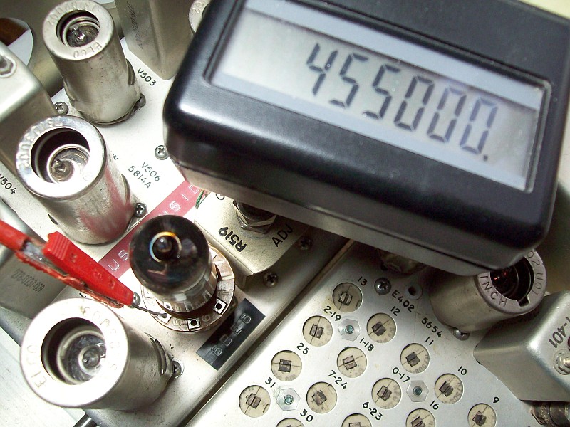
| Product Detectors and Automatic Gain Control for SSB in tube receivers Full SSB integration for the R-390A receiver |
| Preamble:
— AM signal operation:
— Usual SSB product detector operation when it is added to an AM receiver:
|
||||||||||||||||||||||||||||||||||||||||||||||||||||||||||||||||||||||||||||||||||||||||||||
| The so-called product detector:
The product detector is so called because it takes the product of two signals, the sideband signal and the BFO signal, to provide the decoded waveform to the audio amplifier. The output amplitude is the product of the two input amplitudes, so the output voltage depends on the resistive value of the load multiplied by the current and then multiplied by the amplitude of the inserted local signal, hence the name "product". Unlike its use on CW, on SSB the BFO must provide a signal with greater amplitude (output level) than the input signal, but a detail that is often overlooked is that the amplitude of the BFO must be much higher, especially in the case of the passive product detector, however not as much amplitude is needed for the active product detector. In practice, the "product" consists on mixing the sideband with the BFO "carrier" down to the audible range so that the original audio can be heard. This is, the received signal is mixed in some type of non-linear device (active or passive, see below), with a signal from a BFO, to give sum and difference frequencies to the signals being mixed, in the same way that a first mixer stage in a superheterodyne would produce an intermediate frequency, but in this case it is the audio frequency (after filtering out the RF of the sideband and the RF of the BFO). An SSB signal has no carrier, the intelligence is in the transmitted sideband, so a local signal must be added to replace the non-existent carrier. Operationally, the product detector is an electronic circuit that "reassembles a carrier" into a SSB signal so that it can be detected. The mixing (or product) of the SSB signal with the BFO signal is called product detection, but in fact it is a heterodyne detection. Unlike the AM detector, that converts the envelope of the signal into a decoded waveform, the product detector handles the product of two signals to provide the decoded waveform. |
||||||||||||||||||||||||||||||||||||||||||||||||||||||||||||||||||||||||||||||||||||||||||||
Product detector designs with active mixing: Double triode (left), heptode 'pentagrid' (right). 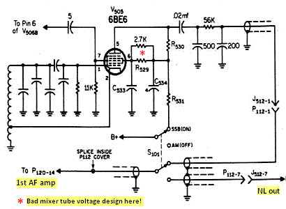 Product detectors with active mixing: These circuits work as mixers/converters, their main advantage is that they do not need large BFO injections... if the circuit is well designed (*). It is necessary that the converter tube operate at the voltages/environment that make it a true converter tube, otherwise it will become a variant of a passive product detector, thus requiring high BFO signal injection. When the tube is acting as a true mixer tube the tuning operation is not critical, the SSB tone change is relatively smooth. The circuit on the left is the heir to Crosby's original circuit and is applied to many Hammarlund receivers and to pre-S line Collins receivers. The circuit on the right is the usual receiver mixer/converter layout applied to a product detector function; but it's a pity that the DC feed on pin 6 has a significant error, probably due to the misunderstanding of associating higher voltage with higher performance. In a mixing tube, increasing the voltage from a point does not increase performance, but rather decreases it; therefore to perform active mixing, 6BE6 must work with mixer tube parameters. (*) If not, a higher BFO output is required. Tubes do not have a life of their own, the “life” they may have is received from the circuit that surrounds them, therefore the connections and the voltages they receive must be consistent with what they were designed for, otherwise a tube will not fulfill its function. |
||||||||||||||||||||||||||||||||||||||||||||||||||||||||||||||||||||||||||||||||||||||||||||
"Product detector" designs with passive mixing: Double diode (left), CW-style diode (right).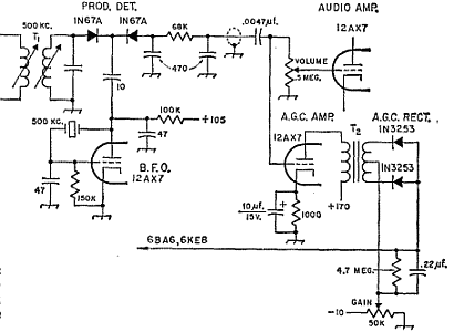 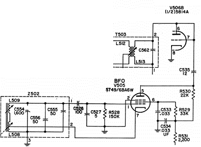 "Product detectors" with passive mixing (note the quotation marks): These circuits work well, but require precise operational settings. They also need a high level of BFO injection (it is in these circuits where the BFO signal must be at least 10 or 20 times the amplitude of the incoming signal). In fact there is no specific 'product detector circuit', these are circuits that promote signal mixing. The circuit on the left is the Miser's Dream1 receiver's product detector with its associated audio AGC circuit, and on the right the R-390's CW-style diode mixer, which is the classic BFO and AM detector that beats signals, it uses the same principle of passive SSB detection if manual control of the mixing process is mastered. Clarifications: — Active: The circuit handles an AC signal driven by DC voltages that establish the AC operation of the circuit. — Passive: The circuit handles an AC signal driven by its own AC potential. DC voltages, if present, do not act on the main function of the circuit. |
||||||||||||||||||||||||||||||||||||||||||||||||||||||||||||||||||||||||||||||||||||||||||||
| ⥤ A combined AM/SSB detector for the R-390A receiver ⥢ No extra switching or rewiring is required - includes noise limiter operation on SSB |
||||||||||||||||||||||||||||||||||||||||||||||||||||||||||||||||||||||||||||||||||||||||||||
|
Background:
This detector circuit combines two classic circuits: the AM detector (original R-390A circuit slightly tweaked) plus the redesigned front-end mixer circuit used in commercial receivers ("the first detector", as it was called in the 1920s and 1930s). The use of the 6BE6 mixer tube as product detector is probably the best option for R-390s, it will require minimal socket pin changes and 6BE6's efficiency is fully proven in a variety of applications. The reputation for being noisy comes more from bad designs that do not respect its mixing function than by its own mixing tube noise; in fact, any noise coming from the 6BE6 itself is far exceeded by the noise coming from the antenna. There is also the option of using a dual 7-pin triode, but the tube available may not be appropriate for that application and frequency (e.g. 6J6). There may be other solutions, one of them, which has been little explored, is to de-convert V506B (the AM detector "diode") from an artificial diode to a real triode (V506B is = 1/2 of 12AU7 = 6C4) and design a triode plate detector circuit, this type of detector can work both as an envelope detector and as a product detector; Collins' last designs were of this type. A very popular Ham design of the mixing tube type product detector is that of P. H. Lee, W3JHR (schematic at very top, on the right), that requires additional switching. Also, the value of the screen grid resistor feeding the local oscillator 'plate' is incorrect, that low value unbalances the voltage distribution of the 6BE6 tube as an active mixer (it seems that value has been sounding out using shunts). In the product detector described here (schematic below), the design value of the screen grid resistor for a 6BE6 operating as a mixer (22 Kohm at about 250 B+) is respected, allowing the "oscillator plate" (that screen grid) to operate at 100 volts, and this allows the 6BE6 plate to reach 150 volts; a very good voltage distribution for a mixer tube. |
||||||||||||||||||||||||||||||||||||||||||||||||||||||||||||||||||||||||||||||||||||||||||||
The OTTTsite Product Detector for R-390A:
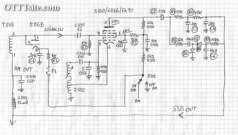
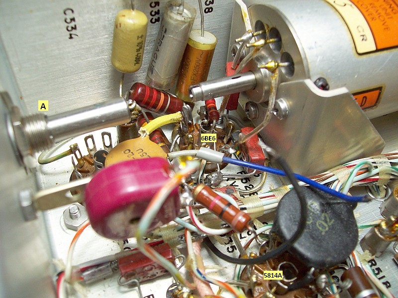
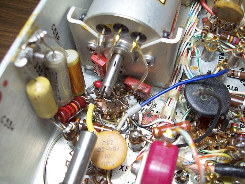
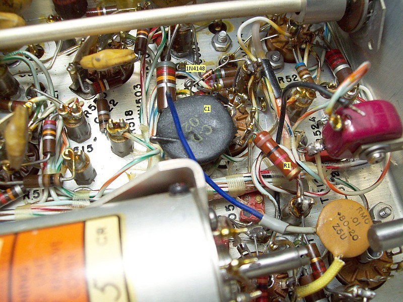
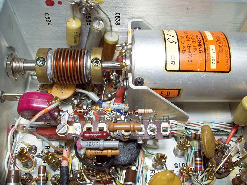
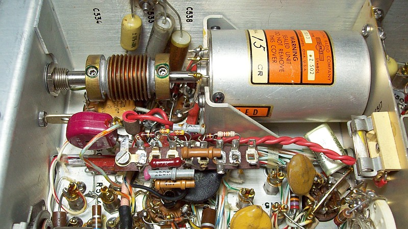 Hover over image to see subchassis from the outside. IMO tube circuits that need modifications should have modifications with tube circuits, so there are no transistors or integrated circuits here. This product detector is designed with that intention and focused on being as “complete” as possible, that is, trying to avoid the situation of improving “x” to worsen “z”, or leaving aside functions of the original device. Therefore, it does not have the classic additional frying noise that is usually produced by excess of BFO injection or by lack of RF filtering (not to be confused with the slight "hissing" sound in the background produced by the Upper/Lower off-center BFO beat). When the product detector is ON the only consequence is that the BFO signal is inserted into the circuit. Its main advantage, which allows total integration, is that the AF output is connected to the general AM signal line and the AM detector is electronically removed from the circuit. This is what makes it possible to fully integrate a product detector into the original R-390A design. SSB signal detection is done easily and without any strange additions to the circuit (e.g. switches, relays). That is, since the main signal line is used in both AM and SSB, all the circuits that operates in AM mode will operate in SSB mode, and as on SSB the AM detector is out of circuit, no additional switching or rewiring is required. The result is that when AM reception is selected, R-390A is a dedicated AM receiver, and when SSB reception is selected, R-390A is a dedicated SSB receiver... all that combined with the AGC circuit of course... since installing a product detector in a receiver without taking into account that its operation must be completed by adapting the AGC circuit is no use... unless the AGC is switched off... but to operate AGC OFF it is not necessary to install a product detector. To control the level and pause of SSB signals, this design has been combined with a well-known mod of the AGC source. It is important not to confuse the functions of a detector circuit with the functions of an AGC circuit, or mix them up. The function of a detector circuit is to offer at its output a quality AF signal for a minimum and maximum input level, that is, if the input level is not between these margins the quality will be compromised, but that will not be the fault of the detector circuit, the fault is that the input is not correct, and the circuit that must adjust the correct input is the AGC. The quality of a detector circuit is checked by placing a medium-to-high level signal at the input; if audio quality is satisfactory, the detector is working OK. The function of an AGC circuit is to maintain the signal level within certain ranges, which should coincide with the input ranges of the detector. Thus, if the detector circuit has been shown to correctly process medium-to-high signals, any demodulation defects are no longer attributable to the detector, but to the AGC which does not allow the signals to be delivered to the detector within the correct level range. The manual signal level corrector is the RF gain control. Therefore, when a detector circuit is modified, the job is not over, the AGC circuit must be checked and, if necessary, adapted to the new detector; that's why I include both circuits on this page. In an AM receiver, adding only the product detector is not enough because on SSB the AGC circuit is more important than the product detector due the AGC circuit ensures that the SSB signal level is appropriate for the BFO level. Some points to keep in mind when repairing and adjusting:
|
||||||||||||||||||||||||||||||||||||||||||||||||||||||||||||||||||||||||||||||||||||||||||||
| Features and description:
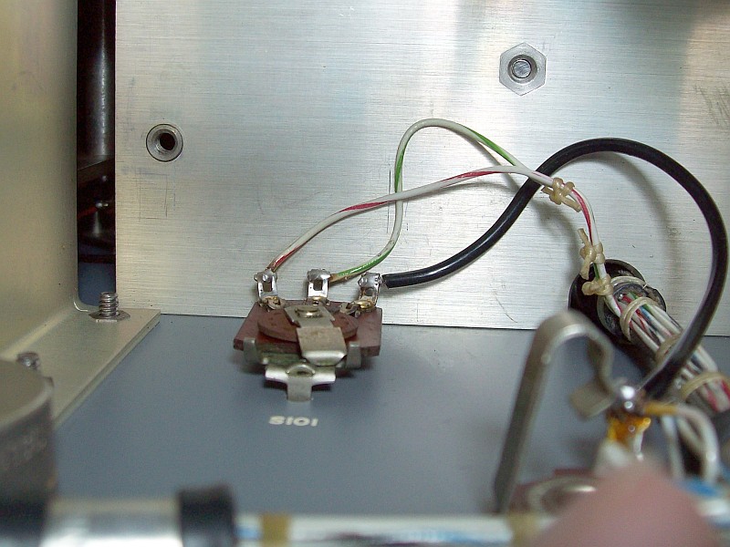
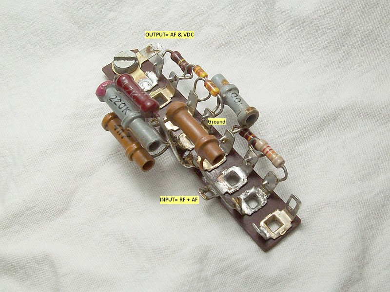
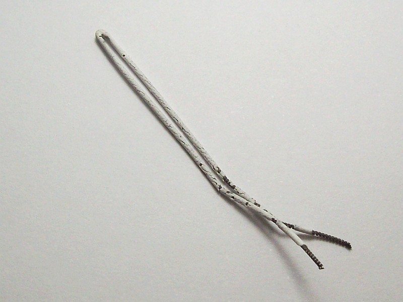
The key to combining the detectors is that the AM detector tube operates also as an electronic switch activated by the free tab of the original S-101 switch. The circuit arrangement to turn the AM detector into a switch implies that on AM the cathode of the detector will have a certain positive bias depending on modulation peaks (100 mV average), this is caused by the 1 Kohm series resistor, but since the signal level on the AM detector plate is high, the practical effect of this positive delay bias at the cathode is irrelevant. On SSB the AM detector is electronically removed by injecting a strong positive voltage into its cathode which completely blocks operation (normal operation implies that the plate must have a higher positive potential than the cathode). Since the AM detector disappears from the circuit, the product detector is inserted in its place. This feature allows another advantage: it is not necessary to replace the original BFO switch. The additional switching circuit to give the AF output, that is common to all product detector designs, is here performed by the AM detector diode (V506B tube). As a final refinement and safety protection, a filament-to-cathode insulation failure protection fuse has been installed for the V506B tube. Adding this fuse is not mandatory but is advisable to avoid a possible failure of the filament-cathode insulation (see table above). The original BFO switch (S101) already provides an easy connection to ground by using the switch tab left free in the original design. This BFO ON/OFF switch circuit is very simple: In the ON position, the B+ line of the product detector is connected to the B+ line of the receiver, and in the OFF position the B+ line of the product detector is connected to ground, and at the same time, this position inserts the AM detector into the circuit instead of the product detector. The R-390A noise limiter operates at a certain bias voltage which represents its working threshold when operating alongside a carrier (see HC-10 A-mod and 75A-4 "squelch" effect). If a standard product detector is used, it will need some assistance in the SSB position because this position will not provide the negative voltage present in the AM position. Therefore, in the product detector described here, in addition to the RF filtering required at the output of a standard product detector, a bias voltage relative to the product detector output level (signal or noise) is added for use by the noise limiter. Both the RF filter and the bias source form a "Bias Tee circuit" which provides AF output to the audio line and -VDC bias output to the NL (the method used here is to rectify the processed IF signal at the output of the product detector before RF filtering). The noise limiter now works identically on AM and SSB, but on SSB, since noise is masked by the action of the product detector (as usual), the NL will only be clearly effective when the noise level is above the signal level.4 |
||||||||||||||||||||||||||||||||||||||||||||||||||||||||||||||||||||||||||||||||||||||||||||
|
The mod has been made with recycled, but tested, parts. This mod does not claim to be perfect, just efficient and adaptable to a very high degree, and it succeeds without a hitch. |
||||||||||||||||||||||||||||||||||||||||||||||||||||||||||||||||||||||||||||||||||||||||||||
| ⥤ Adapting the R-390A AGC voltage source for SSB operation ⥢ The Lankford 2-diode mods |
||||||||||||||||||||||||||||||||||||||||||||||||||||||||||||||||||||||||||||||||||||||||||||
| Background:
About RF gain operation: It should be noted that the AGC circuit that allows a kilowatt neighboring signal and a very weak distant signal to be received without adjusting the RF gain control is usually a fantasy with tube technology (a fully effective circuit would take up too much space). Adjusting RF gain is not only not wrong but perfectly natural, what is not natural is having to adjust it continuously, and to avoid that there is the AGC circuit. The integrated product detector shown above adds VDC to its AF output to match the operation of the R-390A AM detector, but R-390A also has independent AGC source. If the AGC voltage source were the AM/SSB detector, no further work would have to be done since "a carrier" would have been added to the AGC circuit (the HQ-160 link below explains the entire procedure in depth). The R-390A's dedicated AGC circuit (shown below) is "AM style" so something needs to be done to make it handle SSB signals. Due the 'a' and 'b' characteristics of the SSB signals that are described in the Preamble, an AGC line designed for handling AM signals will need modifications to handle SSB signals. There may be several points of view to deal with this, I've developed the one that was applied to the HQ-160; however, it is more common to insert time constants in the AGC line to control the 'a' and 'b' characteristics, which produce the so-called "AGC line pumping" effect. The peculiar control of AGC time constants in R-390A (see S107 switch, schematic below):
The R-390A AGC circuit mod shown below was designed by D. Lankford5 and was based on a previous mod by H. Cornelius (see Hollow State Newsletter issue #1). The way Lankford applies the Cornelius mod was graphically described by himself on HSN #10 (page 3), and this is the origin of some misunderstandings on the authorship of mods. Lankford's own mod was first published on issue HSN #23 (page 4). Later, on HSN #27 (page 8), the mod was discussed in a very scattered text resulting in the version #2 schematic (mouseover below). Dallas Lankford's ingenious mods to adapt the R-390A AGC to SSB. Hover over the schematic below to see Lankford's 2nd design.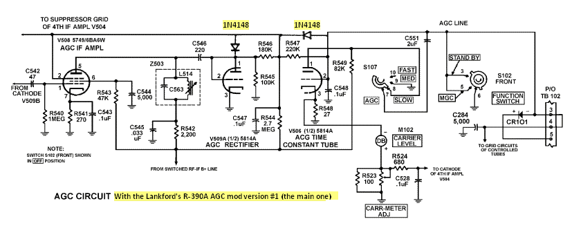 The main change with the first mod is that in the second mod (mouseover) the classic time constant design procedure (passive control) is used; therefore, in SSB position, the 'feedback style' of the original R-390A AGC source design is removed. OTTTsite adaptation of the Lankford 2-diode mod: 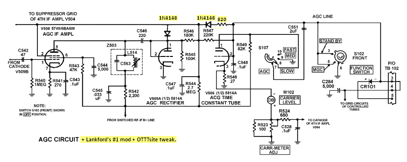 The AGC source circuit above is the current one in operation. As I think that the peculiar Collins time constant circuit should be maintained, the circuit applied is Lankford's mod #1, but modified with a voltage transition safety provision in the diode associated with the C551 discharge (820 ohm resistor, see it above). It is not mandatory to add this resistor, but recommended in order to avoid damaging the diode by accumulation of voltage transition sessions when entering or exiting the SLOW position. One way to detect potential damage to the diode is to see if the "silence time" from SLOW to MED has changed to one second or is even getting faster. This may be interpreted as a happy improvement, but it is not, it means the diode has lost, or is losing, reverse resistance; the consequence will be the popular "pumping effect". As noted above, the R-390A AGC circuit has a very popular 2-second "moment of silence" when switching from SLOW to MED (the other combinations don't produce "moments"). There are Ham circuits that aim to delete or reduce this "moment", but IMHO it is not necessary to complicate things with something that is perfectly bearable, since the change from SLOW to MED is not done continuously, it is only done when changing reception mode. The R-390A AGC circuit also has another "feature": A voltage dump when switching from MED to SLOW which causes an instantaneous sensitivity boost effect, but it lasts only a little more than an instant, so it is totally bearable as well. Precisely, the 820 ohm resistor in series with the 1N4148 diode next to the C551 2 µF capacitor is included in order to protect this diode from the transients of those two events. And finally, there is also a very widespread, more or less obvious, feature present in AGC systems: when selecting a slower time constant, the audio level decreases a little. IMHO trying to design the 'perfect circuit' only leads to endless add-sub designs, which makes what is gained on one side is lost on the other. The usual tactic in SSB AGC design is to control the input impact (attack time) of the signal by acumulating voltage and then maintain a decreasing AGC level by slowly releasing the previously acumulated voltage (release time). The Lankford mod of the R-390A AGC source circuit can be considered an excellent choice to complement the integrated product detector because it is fully in line with the approach taken into account in its design (ease, efficiency, practicality). What this mod does in practice is that when an SSB signal comes in, the diodes bypass the resistors lowering dramatically its value when the generated AGC voltage is above the contact potential (an AGC delay), thus obtaining increased AGC voltage. The receiver then "interprets" that it is receiving a higher signal, and the AGC reacts by lowering it, thus stopping the "hit" of the SSB signal... but on AM this will happen continuously, so the AM reception level will be affected. This is what it means "improving x to worsen z", however, this side effect on AM is bearable, especially if the enormous simplicity of the mod is taken into account, therefore, it is perfectly installable even if not considered entirely adequate (in fact, the Lankford 2-diode mod is a very ingenious 'hack' of the AGC line... using run-of-the-mill diodes!!! )6. Notes and citations:
(1) From the golden age of amateur radio: "Some thoughts on home receiver design", Byron Goodman W1DX, QST May 1965, page 11. "The Junior Miser's Dream", The Radio Amateur's Handbook, page 124, ARRL 1966. A stroke of genius in tube circuit design.
(2) e.g. Increasing the BFO level when what you need to do is decreasing the input signal level, or do something similar by adjusting the input signal coupling to the product detector instead of adjusting the AGC level. If the product detector works OK for medium-to-high level signals, you don't need to tweak it any further. This is where RF gain control comes to the rescue, as it means that the input signal is outside the limits of automatic control. (3) A classic example of this would be the typical mods in audio stages. All manufacturers knew very well how to design audio stages for communications receivers; here, too, each person's hearing plays a role. (4) The R-390A Noise Limiter processes the noise after detection, not before (such as limiters in the detector or in an IF stage). When the NL is ON, the 'overall audio level' drops because noise peaks are excluded from the audio stream. On SSB, the best noise removal action is achieved with the NL set to minimum (to avoid distortion) combined with a high-cut audio filter. (5) Dallas Lankford was one of the editors of Hollow State Newsletter (1983-2000). The HSN was originated as the R-390 user's group that was part of the 80's/90's "boatanchor" boom, this group contributed to popularize the R-390A receiver. (6) To understand the functions of the diodes, it is recommended to read sections 1, 2 and 3 of paragraph (b. Delayed AGC) on page 70 of the TM 11-856A manual (or page 33 of the TM 11-5820-358-35 manual). The delay voltage is located at the junction of R544 and C547, so this positive voltage is present at the junction of R546 and R547 and at the suppressor grids of V504 and V508, neutralizing any contact potential voltage. The negative voltage created by the received signal on the grid of V506A and the plate of V509A combines with this positive voltage at the junction of R546 and R547, creating a delay lag by voltage. On SSB, time constant circuits must charge their capacitors quickly, but resistors limit the charging rate. The diodes remove the R546 and R547 resistors in the charge cycle (attack) bringing the AGC voltage to full level as quickly as possible, and the reverse resistance of the diodes in the discharge cycle tends to maintain the original release characteristic of the circuit. It should be noted that Lankford's modification affects delayed AGC operation, and on AM the circuit will also operate in the same way, it is necessary to ensure some AM compatibility; but the design is so ingenious that its advantages far outweigh its disadvantages. R-390A related info:
|
||||||||||||||||||||||||||||||||||||||||||||||||||||||||||||||||||||||||||||||||||||||||||||