Info about this model 's capacitors.
There are NO waxed paper capacitors in this model, and the existing electrolytic filter capacitors are well sized and of good quality; thus if the electrolytics have not dried out due bad location in the chassis or sealing failure (rare), or have not become corrupted due to poor build quality (cheap mfg), THERE IS NO NEED TO REPLACE THEM. This model does not need the application of any "capacitor replacement kit", you would be spending money in vain. BTW, not all, but many of these kits take advantage of the CLICHE belief that the electrolytic capacitors always need to be replaced, this is simply not true, the cliche only holds true for waxed paper capacitors.
Electrolytic capacitors that have NOT experienced overvoltage or overheating are generally in very good condition, but are not YET usable due to depolarization, as it happens when newly manufactured (and before being polarized by the manufacturer). It is the user who damages the electrolytics when plugging in the device without taking into account this behavior, that is, the user causes the failure at that moment. There is no prior failure since depolarization is not a failure, it is a consequence of the elapsed time. It is disturbing to see that good vintage components go to waste because of a successful cliche, or for ignoring the risks associated with connecting a device that has been in storage for a long time. The consequence is that the original appearance of a device is compromised by totally unnecessary "repairs". I'm posting this warning because it's really disappointing that electronics hobbyists mistake normal behavior for a component failure (or cause the failure themselves).
When depolarized, an electrolytic capacitor is not a capacitor, it is a low-value resistor, but this does't mean mandatory replacement. The thing is: Just like a battery discharges over time, an electrolytic capacitor DEPOLARIZES over time; ALL electrolytics, old and new. This means that before reusing these capacitors after a long time in storage a polarization protocol must be performed. It basically consists of starting the device at reduced voltage, letting time pass, raising the voltage and repeating; a "rinse'n repeat process" until the capacitors no longer heat up. The prize is that it is possible to respect the original design without the need for additional spending, the drawback is that if the capacitor has not been used for many years the process can take many hours, but this should not be a problem for an amateur. See an example of the reforming process on the 75A-4's capacitors page.
About off-tolerance resistors: High impedance electronics, such as tube electronics, are usually very forgiving of component values. Barring large differences or values in critical circuits (e.g. bias), it will normally NOT be necessary to replace vintage resistors.
Purchased on eBay, at first sight it worked fine, only appreciating:
- The very usual dial frequency mismatching along with knob misalignment.
- Band .54-1.32 muted sporadically just when reswitching bands.
- Tuning SSB clear signals in the 27 to 31 Mcs range was very difficult due rough and erratic audio frequency scanning when trying to tune the SSB signal. The problem is increased by the high tuning ratio in that area, adding difficulty.
- A peculiar and erratic behavior: The pilot lamps blinked a bit when scrolling the dial with the Main knob to tune other frequencies. This, to a greater or lesser extent, happened on all ranges. Defective contact in the base? NO.
First, dust was removed with a brush, then removing and washing the knobs and cleaning the front panel. Potentiometer and switch shafts were then lubricated, contact-cleaner spray was NOT used on the band switch in order to prevent dial misalignment due variation of the capacitance (this is usually noticeable in the high frequency range and it is hardly recoverable).
The most obvious fault was sought (sporadic failure in the .54-1.32 band), discovering that the band change switch bar that controls the wafer positions was a bit loose and needed re-tightening, this caused the switch contact to fail. But later, an incremental flaw was discovered; it turns out that the phenolic switch bar has some twist to different degrees depending on the length, this combined with some play in the wafers causes contact displacement and eventually failure. The switch bar must be adjusted by finding a balance point between switch position and contacts; in these long multi-wafer switches this bar should be metallic, or better, also phenolic, but much thicker. See in the 51J-5 (third pic) how Collins solved this problem by using much thicker phenolic bars to move the switch wafers.
Planning the overhaul. The first step should always be to check what is on the table:
- The accuracy of the xtal calibrator (100 Kc) was checked first via capacitive coupling to a digital frequency counter, then was used to achieve maximum S-Meter deviation with the Q-multiplier ON/OFF; but it is better to adjust the Q-MULT when the rest of all adjusts were done; Q-MULT must be adjusted/located at center-resonance of the IF bandpass.
- With the help of an RF generator the resonant frequency of the IF chain was determined and the central position of the CW PITCH control was adjusted by the zero-beat procedure (position CW/SSB). This adjustment must always be made to the narrowest possible bandpass (SELECTIVITY advanced, peak resonance adjusted with FREQ).
- It turns out the low IF was adjusted from factory to 457.2 Kc instead of at the nominal design frequency of 455 Kc; this is totally true since this HQ-160 was undisturbed, the red sealing on the coils of the RF block was intact. That frequency shift in a receiver without a crystal filter in the IF chain is not a problem if the previous RF stages take this difference into account. These IF changes in multiple conversion receivers are very common, may be caused by nominal frequency shifts in the LO crystals of the previous conversion stages or an IF accommodation to the nominal frequency of a crystal filter, but they are also caused by the discrepancy between the actual frequency and the frequency marked on the dial of the generator with which it was aligned.
- Using a RF generator, dial marking is checked, as well as the start and end of each band; usual frequency shifts are observed concluding that this receiver is a good candidate for optimization; the circuit should be analyzed, and finally, an alignment process must be planned.
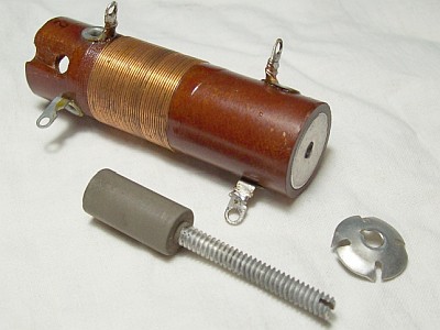
- While designing possible modifications, some dial calibration was carried out retouching the local oscillator with hairlines at center. Initial and final dial frequencies were checked with an RF generator, zero beat tested setting FUNCTION to CW/SSB with CW PITCH at center. The adjusting procedure on each band is the usual: first the low side acting on the oscillator coil slug, after the high side acting on the trimmer. Upper range adjustment of the 3.2-5.7 band is made up of a trimmer and a negative temperature correction capacitor N750 of 1.5 pF (C82) in parallel leaving the trimmer completely open. Adding capacitance to a trimmer using a compensated temperature capacitor is a good idea but it is mandatory to allow enough margin for adjustment for the trimmer, also the fixed capacitor added must have enough capacity to take effect in the circuit, C82 is useless, the effect of a compensated capacitor of 1.5 pF at 5.7 Mcs is minimal, therefore, the most practical is remove it adding those 1.5 pF in favor of the C64 trimmer. Without this capacitor there is one and half slug trip to reach minimum capacity limit, which allows fine adjustment in the high end of that band. After adjusting low / high sides, dial marks must be tested in 100 to 100 Kc steps to see displacements and coincidences, ending with a final adjustment taking into account these displacements in order to obtain a more or less homogeneous overlap on the whole excursion.
- No antenna connected, several coupling points were found in the low range of the 18-31 Mcs band when the ANTENNA control is being tuned for maximum sensitivity. The 6BA6 tube has a 22 ohm grid neutralization resistor (R1), this value was increased up to 82 ohms and couplings disappeared. A receiver must be totally stable, connected or not to an antenna, and in all frequency ranges.
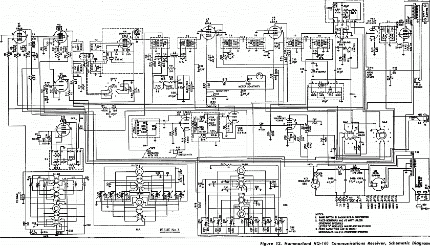
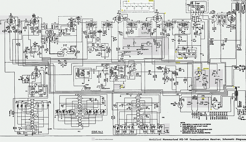
- Main secondary winding voltage in the export version transformer is 310-0-310 AC that results 325 volts at the input of the smoothing filter, due this the V10 plate (6AQ5) works at 325 volts, grid screen just below. This is excessive even though the designer has taken precaution on increasing value of the cathode resistor to limit intensity. It is not healthy for the 6AQ5 tube operate at so high level, thus a combined wiring modification has been made to reduce voltage to the 6AQ5 tube. The first section of the smoothing filter works now only as a voltage reductor, but unfortunately it is not possible to carry on with the filter reactor as the first component of the smoothing filter since it has not enough wattage to support this new configuration, therefore circuit locations of the choke inductor and filter resistor has been exchanged in order to combine wattage with voltage. Current settings are: 325 volts at the input of the smoothing filter (A), 275 volts at the output of the voltage reduction section (B), 245 volts at the output of the smoothing filter (C).
- The BFO B+ line does not have a decoupling network, therefore some BFO RF circulates in the B+ line to be decoupled to ground through the PS capacitors (the same path of the "motor-boating" issue). A capacitor (CD) is installed from the B+ terminal of the BFO to ground to prevent a sporadic parasitic AF beep that self-starts randomly caused by lack of decoupling network in the B+ line of the BFO stage
 . A value of .330 µF at 455Kc represents only 1 Kohm of reactance to ground, this high value is chosen to avoid including the usual network decoupling resistor, thus avoiding voltage drop in the BFO. . A value of .330 µF at 455Kc represents only 1 Kohm of reactance to ground, this high value is chosen to avoid including the usual network decoupling resistor, thus avoiding voltage drop in the BFO.
- Looking inside, a blackened RF decoupling filter resistor (see pic below) in series with the mixer transformer T1 and the plate of the mixer tube V2 (R12, 2K2 ohms) was replaced; but the story doesn't end here, this is the usual clue that implies the so-called silver mica disease. The capacitance loss was compensated for by a previous owner by tweaking the corresponding slug on T1 as the small capacitance involved can be recovered by adding inductance, it works, although of course the resulting Q is not the same.
- Finally, after making the planned modification (see previous page) and solving unexpected issues (SMD, parasitic oscillations, RF coil, band switch bar, IF discrepancy...), this receiver has been fully aligned to meet the design nominal IF of 455 Kcs, and at the same time, it has been taken as a model to explain in great detail the entire tuning process and possible problems that can arise on aligning receivers of various conversions. A detector probe signal pick-up terminal for IF alignment has been installed at the absolute end of the IF chain, the T8 green dot lug. The precision adjustment of an HQ-160 and similar receivers can be consulted in the ES section of this website.
The case of bad SSB reception in the 18-31 band, blinking pilot lamps, & the mysterious 15 Pf capacitor.
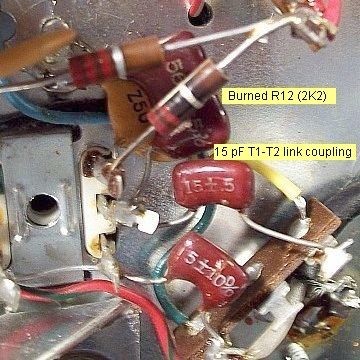 Rough SSB reception on the high end of 18-31 Mcs range (like gargling, 11 & 10 meters bands) is the main problem of this receiver. Rough SSB reception on the high end of 18-31 Mcs range (like gargling, 11 & 10 meters bands) is the main problem of this receiver.
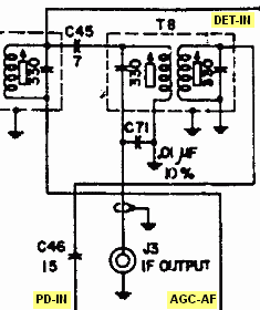
Stability on this range is critical, and any kind of problem can seriously affect signal processing at the demodulator. It seems that Hammarlund spotted this issue and they believed the problem was in the mixer/converter (double conversion) stage. I'm guessing that the 15 pF capacitor in series with the T1-T2 coupling link (see pic at left) was an attempt to correct this issue. This capacitor is from factory, missing in schematic diagrams of this receiver (nor documented as a modification), its inclusion cause weak coupling on double conversion bands, thus lowering sensitivity.
This capacitor does not solve the demodulation problem since SSB distortion is not caused by an excessive input to the mixer/converter circuits or a Local Oscillator issue; the origin of distortion is parasitic oscillation in the RF amplifier to the mixer circuit that uses the tandem capacitors metal cover as resonant path for the parasitic feedback loop. Also, the pilot lamps start blinking on some tuning changes who have the ability to put "the transmitter on". Its leads, that usually are located over the metal case, act as an "antenna", and the signal "received" may be injected as an "extra" into the filament line. The goal is to remove this oscillation, or stop it just when it starts.
Since the parasitic signal is very high frequency is not too noticeable in low bands, but in the high band it is evident because the signal-received / spurious-carrier difference is much less. In this receiver the tandem capacitors compartment with its cover conforms in practice a resonant cavity, the coil compartment underneath is a compact block that needs the use of long leads. The classic component distribution used should have been revised in order to avoid parasitic oscilations, problems that are not too evident on AM become evident on SSB. To prevent interaction with the filament line, wires of pilot lamps have been relocated to safer position, the S-meter and the V1 - V3 (LO) filaments have been RF-shunted with 10 KpF capacitors. The spurious signal generated by the parasitic loop enters together with the tuned signal into the mixer creating an "encrypted" output signal impossible to demodulate correctly by the product detector. Distorted signals generated by the intervention of spurious 'carriers' are a real nightmare since can be interpreted on different ways. I also suppose that the problem was never solved because production ended (the HQ-160 had few years of life, 1957-59, due the advent of HQ-170 in late 1958).
The clue that the problem was not in the converter (in "Hammarlund language" converter means "double conversion") was that the flickering of the pilot lamps also occurs when scanning bands of single conversion. Noting how the SSB signal is being tuned is helpful: there must be a uniform high-low and low-high pitch variation, with good tone, the product detector will make evident any underlying 'carrier' by strident tones. Another clue to find spurious loops is to hear the sound of the bandswitch, if it produces screeching sounds it is "breaking" the spurious loop when changing bands. In the first review of this receiver, a parasitic coupling was found in the antenna amplifier stage (V1 - 6BA6): cathode resistor (R2) almost touched the output wire of the 6BA6 plate (C9), R2 was moved away from the C9 lead, thus creating enough spacing to remove the parasitic coupling on lower frequencies of the 18-31 range, but it wasn't enough on high frequencies. In the current revision to end the problem, various resistance values have been tested at grid inlet and plate outlet with little success, it was concluded that the cause is circuit design and wiring; the RF stage must to be reassembled or redesigned.
This parasitic feedback gets worse due the use of a RF choke as the load of the front-end stage (there is no RF choke that does not have its own resonances). The use of a choke following the antenna amplifier is usually an economic design due it avoids one switch-wafer, although there may be other design reasons. An easy test to check this issue is to remove the metal cover, then the high pitched rough reception disappears, but this cover cannot stay permanently removed due it supports the pilot lamps, a mixed solution must be implemented. Analyzing the design of the front-end stage of this receiver it is evident it was designed mainly for selectivity, it seems the designer knew that amplification had to be under control to avoid problems (the same thought used in the SP-600).
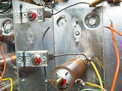
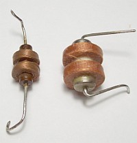 As this problem needs to be eradicated (and the font-end stage can be improved) the redesign was adopted. To do this, the 6BA6 tube was replaced by a 6BZ6 which is a true high-frequency tube, and therefore has a pin distribution designed for this purpose: Control grid and cathode pins are located in the socket opposite from screen grid and plate pins, this allows for easy input/output shielding. Another difference between 6BZ6 and 6BA6 is that the 6BZ6 suppressor grid is not a wire grid, but rather a pair of plates to control the electron beam. The redesign consists on: changing the cathode resistor to 180 ohms, cathode capacitor to 10 KpF, adding a shield between grid/cathode to plate/screen-grid (see picture below), a 10 ohm antiparasitic resistor at the V2 mixer input grid, a ferrite bead at V1 control grid, and choosing a "correct" inductance value for L1 (this choke determines RF amplification and RF losses, the value must avoid the latent parasitic resonance of the circuit). Applying this redesign with the tandem capacitors cover installed the problem disappears, but the circuit will be always sensitive to the spurious resonance. As this problem needs to be eradicated (and the font-end stage can be improved) the redesign was adopted. To do this, the 6BA6 tube was replaced by a 6BZ6 which is a true high-frequency tube, and therefore has a pin distribution designed for this purpose: Control grid and cathode pins are located in the socket opposite from screen grid and plate pins, this allows for easy input/output shielding. Another difference between 6BZ6 and 6BA6 is that the 6BZ6 suppressor grid is not a wire grid, but rather a pair of plates to control the electron beam. The redesign consists on: changing the cathode resistor to 180 ohms, cathode capacitor to 10 KpF, adding a shield between grid/cathode to plate/screen-grid (see picture below), a 10 ohm antiparasitic resistor at the V2 mixer input grid, a ferrite bead at V1 control grid, and choosing a "correct" inductance value for L1 (this choke determines RF amplification and RF losses, the value must avoid the latent parasitic resonance of the circuit). Applying this redesign with the tandem capacitors cover installed the problem disappears, but the circuit will be always sensitive to the spurious resonance.
→ L1 192 µH original choke (left) replaced by a 1.2 mH choke (right). The original low L1 inductance value already shows the clue that amplification was considered problematic by the designer.
The origin of the parasitic resonance is the tandem capacitors metal cover. For VHF/UHF frequencies this cover is in fact a U "coil" fed in the center with grounded ends, it measures 7 + 18.5 + 7 cm x 25 cm deep. To kill the underlying trend to spurious oscillation this "coil" needs to be removed or neutralized. Cannot be removed as it supports the pilot lamps, then it is necessary "break it" into "pieces" in order to kill spurious resonances / feedbacks. To do this, and taking advantage of existing holes, two fixing clamps have been installed on the back to 1/3 of its total length in order to force the cover make ground safely with the tandems case.
About RF tube candidates: The 6GM6 miniature tube is a well known option, but this tube is already a pure wideband amplification tube, that is, designed to give a lot of gain on a medium-low impedance circuit, which is NOT the case (low plate load; using high gain tubes to compensate the low gain of a circuit designed to obtain wideband is a typical design on TV and FM circuits). All the "improvements" applying TV tubes to circuits with medium-high impedances will fail if the goal is gain, since defective impedance coupling cancels what is gained in amplification. Wideband amplification also introduces noise, and the best way to reduce audible noise is to use narrow band tuning, namely: little HI-Fidelity but much HI-Selectivity. A tube is not a 'plug-in' that changes the operation of a circuit, their performance is related to its adaptability to the expected operation of the circuit, that's why there are so many types of tubes.
New 6BZ6 RF front-end stage
Changes applied to the original 6BA6 front-end circuit to avoid parasitic couplings and to improve HF sensitivity
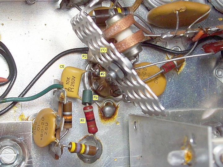
R1 changed to 82 ohms, now pin #2 is cathode, R2 to 180 ohms, C5 to 10 KpF, Fb ferrite bead, (1) I/O shielding.
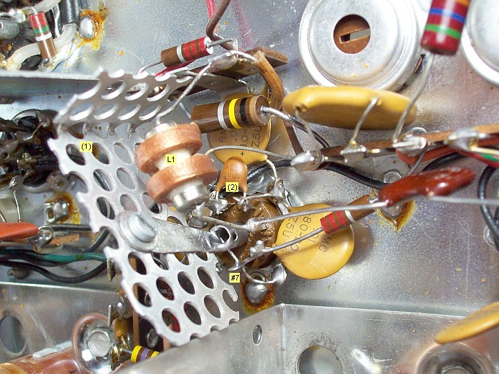
(1) I/O shielding, L1 changed to 1.2 mH, (2) Filament decoupling capacitor, now pin #7 is suppressor-grid.
6BE6 mixer touch-ups and 6C4 local oscillator circuit
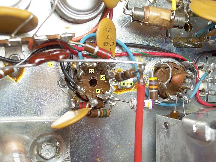
Original wiring design moves away C9 from pin #1 and pin #5, now an antiparasitic 10 ohm resistor is added to pin #7.
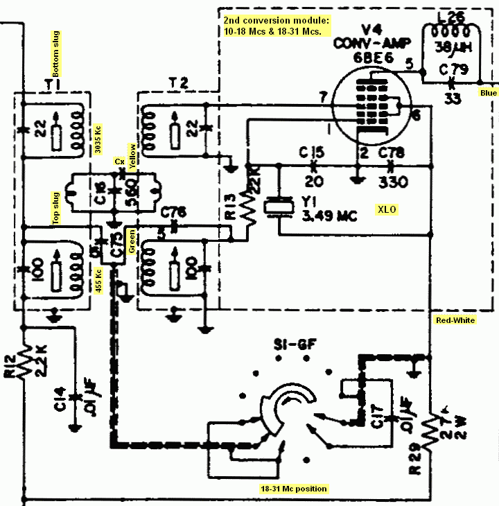
As additional touch-ups the R11 resistor (22 ohms) that, paradoxically, serves to neutralize spurious oscillations, may cause them due preponderant location in the wiring (possible LO harmonic content). This resistor is relocated to a more discreet position (see picture below). Original schematic shows the T1-T2 link (tuned by C16, 560 pF) directly interconnects T1 with T2, thus the mysterious 15 pf capacitor changes total coupling to minimum coupling!!! What problem did Hammarlund want to solve? Isolate mixer from converter? Distortion in the converter when receiving SSB? (that's also one of the things that a good AGC prevents of). There is no distortion in the converter, distortion begins in the front-end due to parasitic oscillation interference as frequency increases. The idea of separating mixer from converter is respected, but instead 15 pF, a capacitance of 820 pF was found more suitable for interlinking T1/T2, low capacitance induce less sensitivity, also an excessive low coupling level favours V4 unstability due lack of damping.
T1/T2 link coupling
Modified T1/T2 schematic area with the 15 pF (Cx) capacitor in the T1 to T2 link + 2nd conversion module.
HQ-160 1st production run: Internals of the 2nd conversion module (note different values for R13 & C78). Courtesy KØCX.
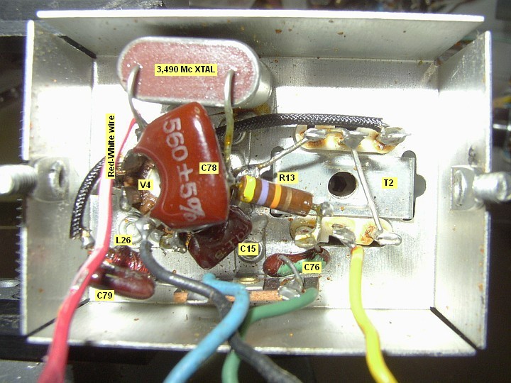
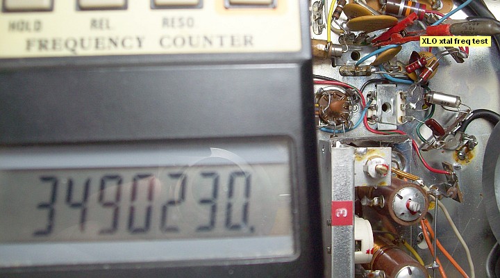
Easy XLO frequency test using a low capacity path: 3,490.230 Kc at the output of the 2nd conversion module.
Changes in the LO to prevent spurious radiation and in the T1/T2 link to improve 10-31 Mcs performance.
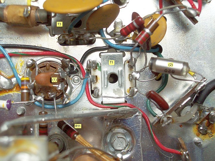
(1) 10 KpF filament decoupling capacitor (2) Adding capacity (820 pF) to the T1/T2 link (15 pF), R11 is relocated inside.
|